FPGA components
Extension — not covered by the 1.0 stability promise (
fpga; the core)
A component with a clock is hardware. You write it as any other component:
ports, variables, functions in the action language, a state machine, test
cases. archec reads the same model three ways. The simulator runs it cycle by
cycle. archec gen --target vhdl writes it as synthesisable VHDL.
archec test --target vhdl runs its test cases on that VHDL, in GHDL.
archec synth synthesises it, places and routes it for a device, and says
what it takes and how fast it runs.
This page builds a PWM generator: a register block a processor writes, an
over-current input that trips the output, and a heartbeat LED. The finished
model is examples/fpga-pwm/main.arche. A second one,
examples/fpga-uart/main.arche, has two clocks: a UART receiver on its own
clock sets the duty cycle of a PWM on another.
What you need#
Writing, checking, simulating and generating need nothing more than archec. Running the VHDL needs GHDL, a free VHDL simulator. Synthesis needs Yosys and nextpnr (where they come from). arche-lang downloads neither.
- In VS Code, install the build of the extension for your machine
(
arche-lang-darwin-arm64.vsix,-darwin-x64,-linux-x64or-win32-x64). It carries GHDL. - Without the extension, install GHDL (
brew install ghdl,apt install ghdl, or a release unpacked in~/.arche/fpga). archec also takesARCHE_GHDL=/path/to/ghdl.
Where GHDL comes from has the versions and the platforms.
1. A component with a clock#
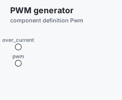
component Pwm "PWM generator" {
  clock clk 100MHz
  reset rst_n active low async
  step tick

  in over_current: bool "Over-current"
  out pwm:         bool "PWM"

  var counter: uint8 = 0
  var periods: uint16 = 0

  fn tick "Every clock cycle"
}
| You write | Meaning |
|---|---|
clock clk 100MHz |
The component is an FPGA component. clk is the clock's name, 100MHz its frequency. Every rising edge is one cycle. |
reset rst_n active low async |
Its reset: a name, active high or active low, sync or async. With no reset line it is rst, active high, synchronous. |
step tick |
The function called on every cycle, as a thread's step is called every period. |
in over_current: bool |
A signal: a port whose type is a data type. |
var counter: uint8 = 0 |
A register. Its first value is its value at reset. |
clock 10ms, with one value, keeps its old meaning: the period of a
component that is not hardware.
Signals and widths#
A port typed with data is a signal of that width. In a body it is a name, as
a variable is: an in signal is read, an out signal is assigned.
| Type | Width |
|---|---|
bool |
1 bit (std_logic on the entity) |
uint8, uint16, uint32, uint64 |
8 to 64 bits, unsigned |
int8 … int64 |
8 to 64 bits, signed |
an enum |
the bits its literals need |
type Adc12 = uint16 { bits 12 } |
12 bits: bits on a type gives any width up to 64 |
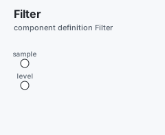
type Adc12 = uint16 { bits 12 }

component Filter "Filter" {
  clock clk 50MHz
  in sample: Adc12
  out level: Adc12
}
An array has a size (var taps: uint8[4]). Floats and strings have no bits:
the checker says so.
Arithmetic means what it means in the simulator. An expression is computed in
full: the sum of two uint8 has 9 bits, and a uint8 less a uint8 may be
negative. It is cut to its width where it is assigned, so a counter wraps. A
shift left stays in the width of what it shifts. A value of a type with
bits 12 wraps at 12 bits, on the simulator too.
Messages#
A port that sends or receives messages stays what it is. Between two FPGA
parts a message is a handshake: valid from the sender with the message's
fields as a record (data), and ready from the receiver.
message PERIOD_DONE "Period done" { periods: uint16 }

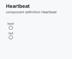
component Heartbeat "Heartbeat" {
  clock clk 100MHz
  reset rst_n active low async
  in beat:   data receives PERIOD_DONE { handler PERIOD_DONE -> on_period }
  out led:   bool "LED"
  var count: uint8 = 0

  fn on_period(periods: uint16) ```arche
    if count == 1 {
      count = 0
      led = not led
    } else {
      count += 1
    }
  ```
}
A sender holds valid until ready. A receiver is ready when it can take
the message: When the receiver is not ready
says when that is. A message port linked to nothing inside is a port of the
top entity. In a test, sent(MSG) counts the messages a link carries.
Registers on a bus#
A memory block with an address is a register the processor beside the FPGA
reaches over the bus. archec writes the AXI4-Lite bank (regmap.md)
and wires it to the component.
component Regs "Registers" {
  clock clk 100MHz
  memory CTRL @ 0x4000_0000 : uint32 rw { enable: uint8 bits "0:0" }
  memory DUTY @ 0x4000_0004 : uint32 rw
  memory STATUS @ 0x4000_0008 : uint32 r
}
In a body CTRL and DUTY are read: the bus writes them (rw, w).
STATUS is assigned: the logic drives it and the bus reads it (r).
2. What it does#
The bodies are the action language, as everywhere. This is the PWM's tick
and its state machine:
const PERIOD = 100
const ENABLE = 1

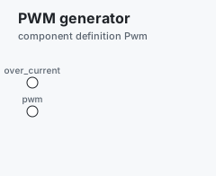
component Pwm "PWM generator" {
  clock clk 100MHz
  reset rst_n active low async
  step tick
  memory CTRL @ 0x4000_0000 : uint32 rw
  memory DUTY @ 0x4000_0004 : uint32 rw
  in over_current: bool
  out pwm:         bool
  var counter:     uint8 = 0

  fn tick ```arche
    if over_current and state != Tripped { goto Tripped }
    if state == Running {
      pwm = counter < DUTY
      if counter == PERIOD - 1 { counter = 0 } else { counter += 1 }
    } else {
      pwm = false
      counter = 0
    }
  ```

  states {
    initial Idle
    state Idle
    state Running
    state Tripped
    Idle -> Running [CTRL & ENABLE == ENABLE]
    Running -> Idle [CTRL & ENABLE == 0]
    Tripped -> Tripped [over_current]
    Tripped -> Idle on "after 1us"
  }
}
What a cycle does#
On each rising edge, in this order:
fn main, when the component has one: its statements up to its nextwait.- Each message taken on this edge: the transition it triggers, the port's
on-receive, its handlers. - The transitions
on "after …"whose time has come. - The transitions with a guard and no trigger. They are tried on every cycle.
- The
stepfunction.
A body reads what it has just written, as in any other component. Outputs are registered: what a cycle computes is seen outside from the next cycle.
Time is counted in cycles#
on "after 1us" is 100 cycles of a 100 MHz clock. A duration that is not a
whole number of cycles is rounded up. Durations go down to the picosecond:
800ps, 6.4ns. fn main runs on its own, and its wait is counted the
same way:
component Blink "Blink" {
  clock clk 100MHz
  out led: bool
  fn main ```arche
    while true {
      led = not led
      wait 500ns
    }
  ```
}
Keep the waits at the top of fn main or of its while true loop. A wait
anywhere else is not synthesised.
States inside states#
A state may hold states, as in any other component. The hardware keeps one
register: the innermost state it is in. The states around it are known from
it, so state == On is true in every state inside On.
states {
  initial Off
  state Off
  state On {
    state Pick { pseudo choice }
    state Heating {
      state Low
      state High
      Low -> High [ticks >= 12]
    }
    state Soak
    Pick -> High [level > 100]
    Pick -> Low [level > 0]
    Pick -> Soak
    Heating -> Soak on "after 100ns"
  }
  Off -> Pick on GO / level = power
  On -> Off on STOP
}| You write | What the hardware does |
|---|---|
On -> Off on STOP |
Taken in any state inside On. Each on-exit runs from the inside out, then the action, then each on-enter from the outside in. |
A transition into Heating |
It enters its first state (Low), or the one marked pseudo initial. |
Heating -> Soak on "after 100ns" |
Counted from when Heating was entered. A change of state inside it does not start the count again. |
state Pick { pseudo choice } |
Left in the cycle it is entered, by its first transition whose guard holds. Give it a last transition with no guard. |
| A transition of the state it is in, and one of a state around it | The one of the innermost state is tried first. |
goto Off in a body |
The same exits and entries as a transition from where it is. |
The simulator and the VHDL run these the same way. A region
(region left), a history state, a fork and a join are not synthesised:
archec check says so. Two regions are two machines: make each a component.
When the receiver is not ready#
A message is a handshake. The sender holds valid and the fields until the
receiver's ready is high on a clock edge.
When a receiver is ready.
| The in port | It takes a message |
|---|---|
has an on-receive or a handler for it |
on every cycle |
| has neither, and transitions are triggered by it | in the states those transitions leave (and the states inside them) |
has depth N |
while it keeps fewer than N. It hands them one a cycle to the rule above. |
component Worker "Worker" {
  clock clk 100MHz
  in items: data receives ITEM
  states {
    initial Idle
    state Idle
    state Busy
    Idle -> Busy on ITEM / take(n)
    Busy -> Idle on "after 40ns"
  }
}
Worker takes an ITEM in Idle. In Busy its ready is low and the item
waits at its sender. With in items: data receives ITEM { depth 3 } three
items wait in the port itself.
What a sender does when its port is full. An out port keeps one message
until it is taken, or depth N of them.
Where the send is |
With no room on the port |
|---|---|
At the top of fn main, or of its while true loop |
It waits. main goes on when there is room. |
Anywhere else: the step function, a handler, an action, inside an if |
The message is dropped. The cycle goes on. |
A dropped message is never silent. The test run says it, on the simulator and in GHDL:
PASS  TP/TC-DROP  A step that sends every cycle
        note: 2 TICK dropped (the first at 30ns): the port they were sent on was full — give it a `depth`, or send from the top of fn main, which waits for room
In a case, dropped(MSG) is how many were dropped: at 1us expect dropped(TICK) == 0. A message a test sends from outside the FPGA
(do send host.port MSG { … }) waits the same way, one behind the other.
3. What cannot be synthesised#
archec check reads every body of an FPGA component as hardware and says
what cannot be made, where it is written:
main.arche:26:12 error f: a floating-point type has no bits to synthesise: use an integer, or a fixed-point value in an integer (millivolts in a uint16) [fpga-synthesis]
main.arche:27:5 error a while loop has no known number of turns, and in hardware a loop runs within one cycle: write `for i in 0..N { … }` with a constant N, or spread the work over cycles with a state [fpga-synthesis]
main.arche:25:15 warning counter is uint8: this value has 12 bits, its top 4 are lost — widen counter, or keep the bits you want (`& 0xFF`) [fpga-width]| Refused | Write instead |
|---|---|
float32, float64, a number like 1.5 |
An integer, or fixed-point in an integer. |
A string, a duration as a value |
An enum or a number; wait and after count the cycles. |
| An array with no size | var buf: uint8[8], or a constant for the size. |
while c { … } |
for i in 0..N { … } with constant bounds, or a state. |
| A function that calls itself | The loop it stands for. |
port.op(…), a call to another part |
A message, or a signal. |
| A Python or TypeScript body | The action language. |
An assignment that loses bits is a warning (fpga-width): a uint16 value
into a uint8, the literal 300 into a uint8. counter += 1 is not one:
a counter wraps at its own width, here as in the simulator. A division by
anything but a constant power of two is a warning too (fpga-divide): it is
synthesised, as a large and slow circuit.
In VS Code these appear in the editor as you type.
4. The system#
component Fpga "FPGA" { kind fpga; chip "LFE5U-25F-6BG381" }

system PwmBoard "PWM board" {
  part fpga:  Fpga
  part pwm:   Pwm
  part heart: Heartbeat
  pwm.beat -> heart.beat
}

deployment OnFpga "On the FPGA" {
  system PwmBoard
  platform PwmBoard
  binary bitstream "pwm_board_top.bit" on fpga {
    thread logic { runs pwm, heart }
  }
}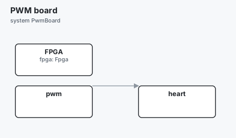
The FPGA parts of a system and its links between them are the top entity. A
port that no link inside drives or reads is a port of the top. The deployment
is optional. With one, a binary on a kind fpga part names the bitstream,
and the top holds the parts its threads run. The chip of the kind fpga
part is the device: archec synth builds for it.
Several clocks#
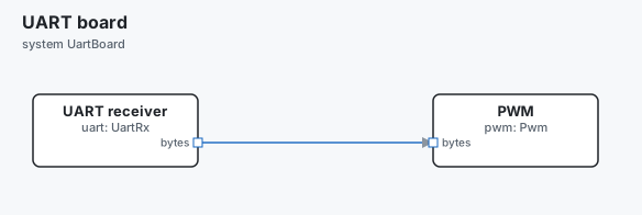
A clock's name is its domain. Parts whose clocks have different names are on different clocks, each a pin of the top:
component UartRx "UART receiver" {
  clock clk_uart 2MHz
  out bytes: data sends BYTE { depth 2 }
}
component Pwm "PWM" {
  clock clk 50MHz
  in bytes: data receives BYTE
}
system UartBoard "UART board" {
  part uart: UartRx
  part pwm:  Pwm
  uart.bytes -> pwm.bytes
}
archec makes each link between two clocks safe, in vhdl/arche_cdc.vhd:
| The link carries | It goes through | What it costs |
|---|---|---|
a bool signal |
two flip-flops of the reader's clock (arche_sync) |
The reader's logic sees a change on its third edge after it. |
| a message | a two-phase handshake (arche_handshake): a request and an acknowledgement, each through two flip-flops; the fields are held still while they are read |
The receiver gets it two or three of its cycles after the sender's edge. The sender's port is free again two or three of its own cycles after the receiver took it. |
A handshake was chosen over an asynchronous FIFO: it is small, it needs no
memory, and it works for any two frequencies. It carries one message at a
time, about one every three cycles of each clock. For more, give the sender's
port a depth: it keeps the burst while the handshake carries it across.
archec check reports the links that cannot be made safe, or may lose
something:
main.arche:42:3 error fast.level -> slow.level goes from clock clk_a to clock clk_b, and level is uint8: its 8 bits do not change at one instant for another clock, which could read a value that never was. Send it as a message (a handshake carries it across), or make it one bit (a bool goes through two flip-flops) [fpga-cdc]
main.arche:43:3 warning fast.flag -> slow.flag goes from clock clk_a to the slower clock clk_b, through two flip-flops: a pulse shorter than a cycle of clk_b (20 ns) can be missed — hold it for two cycles of clk_b, or send a message [fpga-cdc]
The simulator runs each clock with its own period and puts the same flip-flops on each crossing, so a case sees a message arrive on the same edge as in GHDL. All the clocks have an edge at time 0: in a test, the edges of a clock are at whole numbers of its period.
5. Generate the VHDL#
archec gen main.arche --target vhdl -o out| File | What it is |
|---|---|
vhdl/fpga_pwm_pkg.vhd |
The model's data: constants, enums, a record per message, each component's states. |
vhdl/pwm_comp.vhd, vhdl/heartbeat.vhd |
One entity and architecture per component. |
vhdl/pwm_regs.vhd |
The AXI4-Lite register bank of Pwm. |
vhdl/pwm_board_top.vhd |
The system's top: the parts and the bank, wired. |
vhdl/arche_cdc.vhd |
Only with several clocks: the synchronisers of the links between them. |
vhdl/tb/tb_<case>.vhd |
A testbench per test case. |
vhdl/sources.txt |
The files in the order a tool compiles them. |
It is VHDL-2008 with ieee.numeric_std. A component is one clocked process
whose variables are the registers. Each piece names the model element it
comes from:
entity pwm_comp is
  port (
    clk          : in  std_logic;  -- clock clk: 100 MHz
    rst_n        : in  std_logic;  -- reset, active low, asynchronous
    over_current : in  std_logic;  -- in over_current: bool "Over-current"
    pwm          : out std_logic;  -- out pwm: bool "PWM"
    beat_valid   : out std_logic;  -- out beat: sends a PERIOD_DONE
    beat_ready   : in  std_logic;  -- the receiver takes it
    beat_data    : out period_done_t;  -- the fields of PERIOD_DONE
    reg_ctrl     : in  std_logic_vector(31 downto 0);  -- memory CTRL @ 0x40000000: the bus writes it, the logic reads it
    …
-- @arche Pwm.tick main.arche:80 fn
procedure f_tick is -- Every clock cycle
begin
if (over_current = '1') and (v_state /= pwm_st_tripped) then
go(pwm_st_tripped);
end if;
if v_state = pwm_st_running then
v_pwm := resize(v_counter, 32) < unsigned(reg_duty);An entity is named after its component. Here it is pwm_comp, not pwm: a
port has that name already.
Write your own VHDL between the USER CODE markers (Pwm.declarations,
Pwm.cycle, Pwm.architecture). archec gen keeps what is between them when
it writes the file again (regeneration.md).
6. Test it#
The test cases are the model's, written once:
test-plan TP-PWM "PWM generator" {
  case TC-TRIP "Over-current: low, until 1 µs without it" {
    verifies REQ-TRIP
    at 0ns do pwm.DUTY = 80
    at 20ns do pwm.CTRL = 1
    at 200ns expect pwm.pwm
    at 200ns do pwm.over_current = true
    at 210ns expect not pwm.pwm
    at 210ns expect pwm.state == Tripped
    at 500ns do pwm.over_current = false
    at 1490ns expect pwm.state == Tripped
    at 1500ns expect pwm.state == Running
  }
}
archec test main.arche # on the simulator
archec test main.arche --target vhdl # on the VHDL, in GHDLarchec test runs the cases of a system with FPGA parts on the browser
simulator, which steps the clocks (--sim web runs every case there).
archec test --target vhdl main.arche
  GHDL 6.0.0 (llvm jit) — ~/.arche/fpga/ghdl-6.0.0-darwin-arm64/ghdl/bin/ghdl (~/.arche/fpga)
PASS  TP-PWM/TC-DUTY        25 % duty  — 10 expectation(s), 204 cycle(s) of 10ns, 1.2 s
PASS  TP-PWM/TC-TRIP        Over-current: low, until 1 µs without it  — 9 expectation(s), 151 cycle(s) of 10ns, 1.2 s
…
5/5 passed on GHDL

Requirements: 4 verified by passing cases, 0 failing
--plan and --case choose the cases, as for any test run. In VS Code,
Arche: Run FPGA Tests in GHDL runs them and shows the report in the Arche
Status output; Arche: Generate Code… has the vhdl target.
How time is read#
A case is written in time; hardware counts cycles. With a clock of 10 ns the edge at 40 ns is cycle 4. The simulator and the testbench read a case the same way, so a line holds on both, at the same instant.
| Line | What happens |
|---|---|
at t expect c |
The condition is read at t, just after the edge at t if a clock has one there. |
within d expect c |
It is read after each edge of the window, and must hold once. |
at t do part.signal = v |
The input is driven at t. The logic sees it on the part's next edge. |
at t do part.REG = v |
The register is written over the bus. It is in the bank on the part's next edge, and the logic reads it one edge later. |
at t do send host.port MSG { … } |
A message from a part outside the FPGA. It is received on the part's next edge, if its port is ready then. |
Times go down to the picosecond: at 6.4ns, at 12800ps, within 800ps. A
156.25 MHz clock has its edges at 6.4 ns, 12.8 ns, 19.2 ns. A time need not
be on an edge: with two clocks, at 20ns is an edge of one and between two
edges of the other, and each part is read as it is then. A clock whose period
is not a whole number of picoseconds (48 MHz: 20833.333 ps) runs at the
nearest one, and archec check says so.
The bank answers a write before it takes the next: a write takes two cycles. One written too close to the one before waits, on both sides, and the test run says so.
In an expectation you read a part's variables, its signals, its registers and
its state, and sent(MSG). A testbench sets what comes from outside: the
top's input signals, the bus registers, messages from a part outside the
FPGA. A case that sets a variable inside the logic, or is written in Python,
is not run in GHDL. The run says why.
What it proves#
Each case that ran is evidence, at the place ghdl. That is a rung of
the test ladder between the simulator and the
board, and archec test --ladder runs it for a model with FPGA parts:
archec test --ladder main.arche
  ✓ sim     5 case(s) passed on the browser simulator
  – renode  skipped: no deployment with a binary on a board
  ✓ ghdl    5 case(s) passed on the FPGA's VHDL in GHDL 6.0.0
  – board   skipped: no deployment with a binary on a board
✓ ladder: held up to ghdl
$ archec status main.arche
REQ-TRIP Trip on over-current
satisfied by Pwm (pwm)
built into arche-out/vhdl/pwm_comp.vhd:3-4,56-60
highest rung ghdl (sim ✓, renode –, ghdl ✓, board –)
✓ test TP-PWM/TC-TRIP ghdl just now 9 expectation(s) held over 151 cycle(s), GHDL 6.0.0
✓ test TP-PWM/TC-TRIP web sim just nowThe record keeps the hash of the VHDL it ran. Change the model or the VHDL, and the proof is out of date until the case runs again.
Why, and why not#
Each run leaves a trace beside the VHDL, arche-out/vhdl/trace/<case>.trace,
with cycle-accurate times: the states entered, the messages sent and received,
the fields of what came, the sends dropped. A time is in nanoseconds from the
start of the case, with its picoseconds after a point (arche-trace 6.4 send WORD 1). With several clocks they are on one time line. archec why,
why-not and timing read it as they read a firmware's trace
(why.md).
$ archec why main.arche --trace arche-out/vhdl/trace/tp_pwm_tc_trip.trace "pwm Tripped"
pwm Tripped  Running → Tripped: by a goto                   210 ns

$ archec why main.arche --trace arche-out/vhdl/trace/tp_pwm_tc_beat.trace
       0 ns  pwm starts in Idle
      40 ns  pwm Idle → Running [CTRL & ENABLE == ENABLE]  main.arche:108
    1030 ns  pwm sends PERIOD_DONE
    1040 ns  heart receives PERIOD_DONE periods: 1
…
$ archec why-not main.arche --trace arche-out/vhdl/trace/tp_pwm_tc_duty.trace "Running -> Idle"
pwm: Running -> Idle [CTRL & ENABLE == 0]  main.arche:109
  the guard [CTRL & ENABLE == 0] was never true while pwm was in Running (40 ns to 2040 ns): it is tried on every cycle — …
A trace has no values of the variables. archec why-not --test <case> runs
the case on the simulator, which has them.
7. Synthesise it#
GHDL shows the VHDL does what the model says. archec synth shows it can be
built: it synthesises the design for a device, places and routes it, and
measures it.
archec synth main.archearchec synth main.arche
Yosys 0.71+39 with the GHDL plugin, nextpnr-ecp5 0.11.1 — ~/.arche/fpga/oss-cad-suite-20261116-darwin-arm64/oss-cad-suite/bin (~/.arche/fpga)
PwmBoard pwm_board_top on LFE5U-25F-6BG381
LUTs 257 of 24288 1 %
FFs 163 of 24288 1 %
BRAM 0 of 56 0 %
DSP 0 of 28 0 %
pins 101
each component on its own (its ports free: more than its share of the top):
Pwm 526 LUTs, 188 FFs (pwm_comp + pwm_regs)
Heartbeat 14 LUTs, 10 FFs (heartbeat)
✓ clock clk: fmax 123.4 MHz, above the 100 MHz of Pwm, Heartbeat
✓ limit PwmBoard.luts <= 500 257 LUTs <= 500 REQ-FIT
✓ limit PwmBoard.ffs <= 300 163 FFs <= 300 REQ-FIT
✓ limit Pwm.fmax >= 100MHz 123.4 MHz >= 100 MHz REQ-FIT
evidence: 5 record(s) → .arche/evidence/synth.jsonl (archec status)
✓ PwmBoard synthesises for LFE5U-25F-6BG381 and meets its clock, 3 limit(s) keptThe steps are those of any open-source FPGA flow:
- archec writes the VHDL under
arche-out/vhdl, asarchec gendoes. - Yosys reads it through GHDL (the ghdl-yosys-plugin; with a Yosys that has
no plugin, through
ghdl --synth) and maps it to the device's cells (synth_ice40,synth_ecp5). - nextpnr places and routes the top for the device and its package, and reports the highest frequency each clock can run at: its fmax.
- Each FPGA component is also synthesised on its own, with its register bank.
The tools' files and logs are in arche-out/synth/.
The device#
The device is the chip of the system's kind fpga part (its part-number
when it has no chip):
component Fpga "FPGA" { kind fpga; chip "LFE5U-25F-6BG381" }
| Family | You write | Tools |
|---|---|---|
| Lattice iCE40 | iCE40UP5K-SG48, iCE40HX8K-CT256, iCE40LP8K-CM81, iCE5LP4K-SG48; short: up5k, hx8k |
synth_ice40, nextpnr-ice40, icepack |
| Lattice ECP5 | LFE5U-25F-6BG381, LFE5UM-45F-7MG285, LFE5UM5G-85F-8BG381; short: ecp5-25f |
synth_ecp5, nextpnr-ecp5, ecppack |
A name with no package takes the family's usual one (up5k is the SG48). A
device archec does not know is a warning on the chip (synth-device).
--device <name> asks for another device than the model's. Such a run is a
question: it is printed, not recorded.
What it measures#
| Word | What is counted |
|---|---|
luts |
4-input look-up tables. On an ECP5 a carry cell counts for two. |
ffs |
Flip-flops. |
bram |
Block RAMs (4 kbit on an iCE40, 18 kbit on an ECP5). |
dsp |
DSP blocks (a multiplier). |
fmax |
The highest frequency the clock can run at, once placed and routed. |
The cells are Yosys's count after mapping. "of 24288" is what the device has, from nextpnr.
A system's numbers are the top's: every FPGA part, wired. A component's
numbers are of the component alone, with its register bank. Alone, every one
of its ports is free, so nothing is simplified across them: a component takes
more on its own than its share of the top. Here Pwm alone takes 526 LUTs
and the whole top 257. A component's fmax is that of its clock in the top.
Limits in a requirement#
A requirement bounds what is measured, as it bounds a geometry's mass (cad.md):
requirement REQ-FIT "Fits the device" {
  text "The FPGA parts shall take at most 500 LUTs and 300 flip-flops of the device, and the PWM generator shall run at 100 MHz."
  limit PwmBoard.luts <= 500
  limit PwmBoard.ffs <= 300
  limit Pwm.fmax >= 100MHz
}
The name is an FPGA component or a system with FPGA parts. Bound a system for
what the device must hold, and a component to budget it alone. A limit not
kept is an error at its line, and archec synth exits 1:
✗ main.arche:49:3 REQ-FIT: Pwm runs at 35.91 MHz at most once placed and routed; the limit is >= 100 MHzWith no limit written, each clock is still checked against the frequency the
model gives it. A clock too fast for the device is said at the component's
clock.
Four devices#
The PWM generator of examples/fpga-pwm, measured with Yosys 0.71 and
nextpnr 0.11.1 (the default seed), on a Mac:
| Device | LUTs | FFs | BRAM | DSP | Pins | fmax of clk |
At 100 MHz |
|---|---|---|---|---|---|---|---|
ECP5 LFE5U-25F-6BG381 (the model's) |
257 of 24288 | 163 | 0 | 0 | 101, on the package | 123.4 MHz | met |
ECP5 LFE5UM5G-85F-8BG381 |
257 of 83640 | 163 | 0 | 0 | 101, on the package | 175.7 MHz | met |
iCE40 HX8K-CT256 |
183 of 7680 | 163 | 0 | none | 101, on the package | 99.97 MHz | missed by 0.03 MHz |
iCE40 UP5K-SG48 |
183 of 5280 | 163 | 0 | 0 of 8 | 101, virtual | 35.91 MHz | not met |
On an iCE40 the 69 carry cells sit beside the LUTs and are not counted in
them. An iCE40 UP5K is a slow, low-power device: this design runs at about
36 MHz on it, so its clock clk 100MHz cannot be kept there. archec synth main.arche --device up5k says so, at the model:
✗ main.arche:67:3 Pwm's clock clk is 100 MHz: on iCE40UP5K-SG48 its logic runs at 35.91 MHz at most — a slower clock, a faster device, or less work in one cycle (a state more)fmax moves by a few percent with nextpnr's seed (--seed). Keep a margin: a
design at 99.97 MHz for 100 has none.
Virtual pins#
The top of the example has 101 pins: the AXI4-Lite bus of its registers is 96 of them. An ECP5 in a BG381 package has them. A UP5K in an SG48 has 39 pins for you, and nextpnr cannot place the top.
archec then places it with virtual pins. It wraps the top in a module that puts a register in front of each pin, but the clocks and the resets. The inputs become a shift register fed by one real pin. The outputs are folded into a signature read on another. This is what the design sees when the bus master is inside the FPGA (a soft processor, a bridge), not on its pins.
- The cells counted are the design's alone, not the wrapper's.
- fmax is measured with the wrapper. It is a little higher than with real pins, which hold the logic near the edge of the device: 102.9 MHz against 99.97 MHz on the HX8K.
- There is no bitstream of it: it is a measure, not a design to load.
--virtual-pins asks for them on a device where the pins fit.
What it proves#
Each limit measured is evidence for its requirement, at the place
synth <device>. Each FPGA component placed and routed is evidence for the
requirements it satisfies, on the rung synth of
the test ladder, above ghdl:
$ archec status main.arche --req REQ-TRIP --req REQ-FIT
REQ-TRIP  Trip on over-current
  When the over-current input is high, the PWM output shall be low within 2 clock cycles and stay low until the over-current input has been low for 1 µs.
  satisfied by  Pwm (pwm)
  built into    arche-out/vhdl/fpga_pwm_pkg.vhd:17-20, arche-out/vhdl/pwm_comp.vhd:3-4,56-60
  highest rung  synth (sim –, renode –, ghdl ✓, synth ✓, board –)
  ✓ test    TP-PWM/TC-TRIP  ghdl                  just now  9 expectation(s) held over 151 cycle(s), GHDL 6.0.0
  ✓ synth   synth Pwm       synth lfe5u-25f-6bg381  just now  526 LUTs, 188 FFs, fmax 123.4 MHz ≥ its clock's 100 MHz, on LFE5U-25F-6BG381

REQ-FIT   Fits the device
  The FPGA parts shall take at most 500 LUTs and 300 flip-flops of the device, and the PWM generator shall run at 100 MHz.
  highest rung  synth (sim –, renode –, synth ✓, board –)
  ✓ synth   Pwm.fmax       synth lfe5u-25f-6bg381  just now  123.4 MHz >= 100 MHz
  ✓ synth   PwmBoard.ffs   synth lfe5u-25f-6bg381  just now  163 FFs <= 300
  ✓ synth   PwmBoard.luts  synth lfe5u-25f-6bg381  just now  257 LUTs <= 500
A limit kept proves its requirement. A component synthesised does not prove the requirements it satisfies: their tests do. It says the hardware they ran as, in GHDL, can be built for the device and meets its clock. One that does not meet its clock fails them. The record keeps the hash of the VHDL: change the model, and it is out of date. A record for a device the model no longer names is not counted.
When synthesis fails#
archec writes the VHDL, so it synthesises. Your own VHDL in a USER CODE
region may not. The error names the model element the line is of:
✗ synthesis of pwm_board_top for LFE5U-25F-6BG381 failed: no declaration for "no_such_signal"
    main.arche:64  component Pwm (your VHDL in the USER CODE region Pwm.cycle)
    arche-out/vhdl/pwm_comp.vhd:160
    the tools' logs: arche-out/synth/
A run that fails records nothing.
A bitstream#
--bitstream also writes the file to load: arche-out/synth/<top>.bin for
an iCE40 (icepack), <top>.bit for an ECP5 (ecppack). Each pin of the top
must be on the device, so the top must fit the package. Say which pin is
which with --constraints: a .pcf file for an iCE40, a .lpf for an ECP5.
archec does not write it: the store has no FPGA board yet to read the pins
from. With no constraints nextpnr chooses the pins, and the run says the
bitstream is not for a board.
A blinker for an iCEBreaker (an iCE40 UP5K, a 12 MHz clock on pin 35, a button on pin 10, a red LED on pin 11):
component Blink "Blink" {
  clock clk 12MHz
  reset rst_n active low async
  out led: bool "LED"
  fn main ```arche
    while true {
      led = not led
      wait 500ms
    }
  ```
}
component Fpga "FPGA" { kind fpga; chip "iCE40UP5K-SG48" }
system Board "Board" { part fpga: Fpga; part blink: Blink }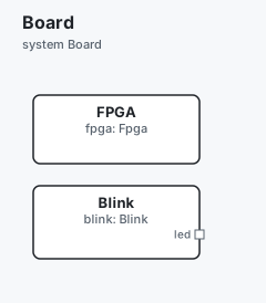
# icebreaker.pcf: the top's ports are clk, rst_n and <part>_<signal>
set_io clk 35
set_io rst_n 10
set_io blink_led 11
archec synth main.arche --bitstream --constraints icebreaker.pcfBoard board_top on iCE40UP5K-SG48
LUTs 39 of 5280 1 %
FFs 25 of 5280 1 %
…
✓ clock clk: fmax 60.08 MHz, above the 12 MHz of Blink
bitstream: arche-out/synth/board_top.binLoading it on the board is yours. With the board plugged in:
~/.arche/fpga/oss-cad-suite-*/oss-cad-suite/bin/iceprog arche-out/synth/board_top.bin(ecpprog or openFPGALoader for an ECP5 board.) This bitstream was built
and packed here. It was not loaded on a board: nothing on this page ran
on hardware, and the pin numbers above are from the board's documentation,
not from a run.
The commands#
archec gen <main.arche> --target vhdl [-o generated] [--deployment D] [--check] [--diff]
archec test <main.arche> --target vhdl [--plan P]… [--case C]… [-o arche-out]
                         [--deployment D] [--json] [--verbose] [--no-record] [--timeout 600]
archec synth [main.arche] [--device <name>] [--system S] [--deployment D] [-o arche-out]
                          [--virtual-pins] [--bitstream [--constraints pins.pcf|pins.lpf]]
                          [--seed N] [--json] [--verbose] [--no-record] [--timeout 900]
archec synth --install-tools [--archive <file>]
archec test --target vhdl exits 0 when every case passed, 1 when one failed,
and 2 when it could not run: no GHDL, no FPGA part, a model with errors. It
writes the VHDL and the testbenches under <out>/vhdl even when GHDL is not
there. --verbose shows what GHDL prints. --json gives the results as JSON,
which are also in <out>/.archec/ghdl-results.json.
archec synth exits 0 when the design synthesises, meets its clocks and
keeps its limits, 1 when it does not, and 2 when it could not run: no tools,
no device named, no FPGA part, a model with errors. Its results are in
<out>/.archec/synth-results.json (--json prints them). In VS Code,
Arche: Synthesise FPGA Design runs it and shows the report
in the Arche Status output.
Where GHDL comes from#
archec looks for GHDL in this order: ARCHE_GHDL (the program, or the folder
a release was unpacked in), the extension's own folder, ~/.arche/fpga
(ARCHE_FPGA_HOME), then the PATH. It never downloads it.
The platform builds of the extension carry an official GHDL release, checked
against its sha256 when the extension is packaged
(tools/fpga/targets.json):
| Build | GHDL | Notes |
|---|---|---|
darwin-arm64 |
6.0.0, LLVM JIT | macOS 14 or later. |
darwin-x64 |
5.1.1, mcode | GHDL 6.0.0 has no build for Intel Macs: 5.1.1 is the last one. |
linux-x64 |
6.0.0, mcode | Built on Ubuntu 24.04: it needs glibc 2.38 or later. |
win32-x64 |
6.0.0, mcode | The UCRT build: Windows 10 or later. |
linux-arm64 |
none | GHDL publishes no build for it. Install GHDL: archec finds it on the PATH. |
These builds need no compiler or linker on your machine. The generic
arche-lang.vsix has no GHDL, and uses the one of the PATH.
To get the pinned release on a machine without the extension:
node tools/fpga/package.mjs --install # into ~/.arche/fpgaGHDL is free software under the GPL (version 2 or later). The extension ships
its release unmodified, beside its own files; fpga/NOTICE.txt says where its
source is.
Where the synthesis tools come from#
archec synth needs Yosys with the ghdl-yosys-plugin, nextpnr for the
device's family, and icepack or ecppack for a bitstream. The
OSS CAD Suite of YosysHQ
has them all in one folder. archec looks for them in this order:
ARCHE_OSS_CAD_SUITE (the folder a suite is unpacked in), ~/.arche/fpga
(ARCHE_FPGA_HOME), then the PATH.
The suite is large: about 500 MB to download, 1.8 GB unpacked. It is in no build of the extension, and archec does not download it: you do.
archec synth --install-tools     # says the file for your machine, and its sha256
curl -fLO https://github.com/YosysHQ/oss-cad-suite-build/releases/download/2026-11-16/oss-cad-suite-darwin-arm64-20261116.tgz
archec synth --install-tools --archive oss-cad-suite-darwin-arm64-20261116.tgz
The release for each platform is pinned in tools/fpga/synth-targets.json
(2026-11-16: Yosys 0.71, nextpnr 0.11.1). The file you give is checked
against its sha256, then unpacked in ~/.arche/fpga, nowhere else. An
archive with another hash is not unpacked.
| Platform | Pinned | How its hash was checked |
|---|---|---|
darwin-arm64 |
yes | Downloaded here, its sha256 computed, the flow run on it. |
darwin-x64, linux-x64, linux-arm64, win32-x64 |
yes | The digest GitHub publishes for the release's file. Not downloaded, not run. |
Tools you installed yourself work too (brew install yosys nextpnr, your
distribution's packages). A Yosys with no GHDL plugin is used with the GHDL
archec finds: the VHDL goes through ghdl --synth.
The suite's tools are free software: Yosys, nextpnr, Project IceStorm and Project Trellis under the ISC license, GHDL and its plugin under the GPL. archec starts them as commands. It ships none of them.
Limits: what it does not do yet#
- Whole picoseconds. The simulator and the testbench count whole
picoseconds. A 48 MHz clock (20833.333 ps) runs at 20833 ps there, and
archec checksays so. The VHDL itself has no period in it. - Between two clocks: one bit, or a message. A signal of several bits is refused: send it as a message. The handshake carries about one message every three cycles of each clock; there is no asynchronous FIFO. In a test all the clocks start in phase, at time 0: another phase is not tried. The simulator and GHDL have no metastability: the two flip-flops are there for the real device.
- States: no region, no history. A state inside a state, its initial child and a choice are synthesised. A region, a history state, a fork, a join, an entry and an exit point are not.
- A port with two senders needs an arbiter of yours: only its first link
is wired.
overflow drop-oldestandoverflow blockare not synthesised: a full port drops the message sent to it, orfn mainwaits. - A message carries fields.
send port MSG { field: value }: a message declared as one value (message LEVEL: uint8) is not sent from a body. - Registers of 32 bits at most from a test. A testbench writes a register over the bus in one AXI4-Lite write, and the bank takes a write every two cycles. A memory block of more than 16 elements is a memory window of the bank, not wired to the component.
- Not run in GHDL: a case that sets a variable inside the logic, uses a
setup, akeyframeor afault, or is written in Python. - Arche's own simulator does not step a clock.
archec testruns the cases of a system with FPGA parts on the browser simulator instead;--sim pythonstill asks for Arche's. - Synthesis for iCE40 and ECP5 only.
archec synthknows these two families, which have open-source tools. For a Xilinx or an Intel device, give the VHDL (vhdl/sources.txt) to Vivado or Quartus yourself. - Pin constraints are yours. archec does not write a
.pcfor.lpffile: the store has no FPGA board to read the pins from. - Never run on hardware. The design was simulated in GHDL, synthesised, placed, routed and packed. No bitstream was loaded on a board.
- A component's share of the top is not measured. Its numbers are of the component synthesised alone.
- Virtual pins on one clock each. A pin of the top is registered on the clock of the part it belongs to. With several clocks the fmax of each is reported.
- No timing constraint between two clocks. A link between two clocks goes
through the synchronisers of
arche_cdc.vhd. nextpnr reports the paths from one clock to another apart: they count in neither clock's fmax, andarchec synthwrites no false-path or maximum-delay constraint for them. The flip-flops carry theasync_regattribute, which Vivado reads; in another tool, constrain the crossing yourself. - The synthesis tools were run on macOS (arm64) only. The other platforms' releases are pinned by the hash GitHub publishes.
- The Windows build of GHDL is pinned and checked, and was not run by the tests of this feature.